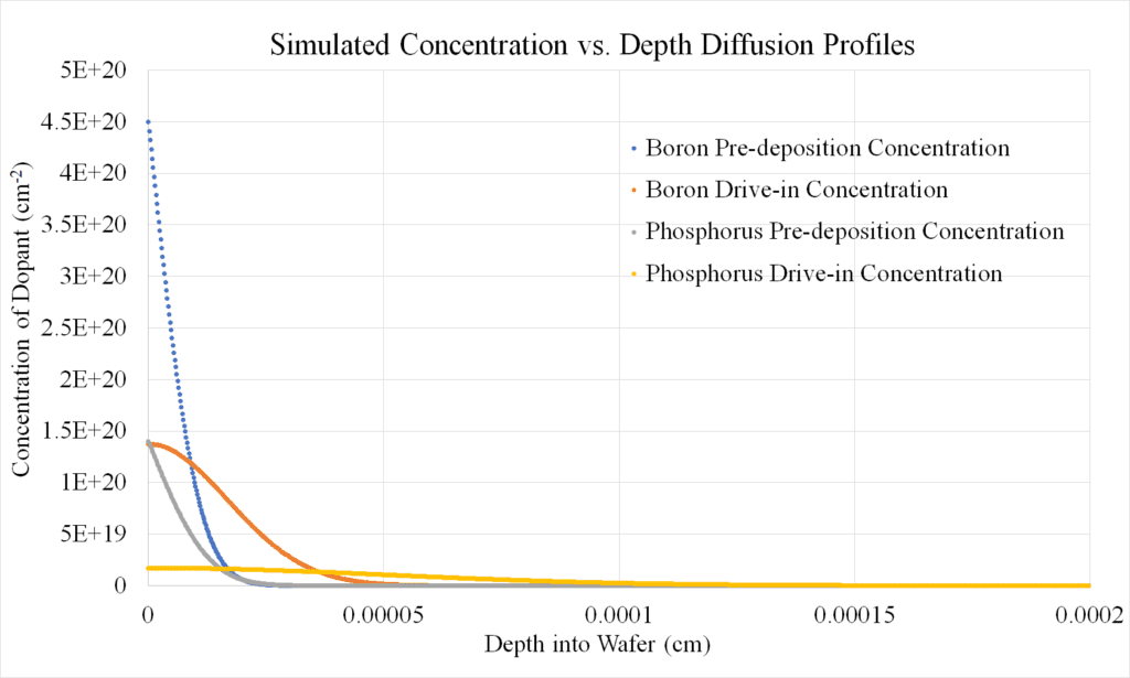


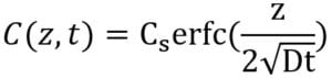
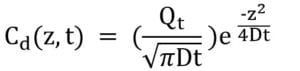
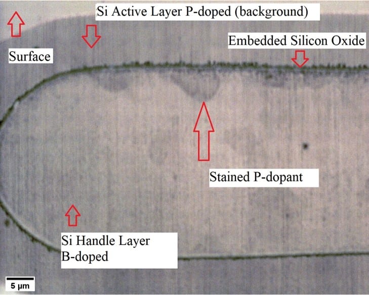
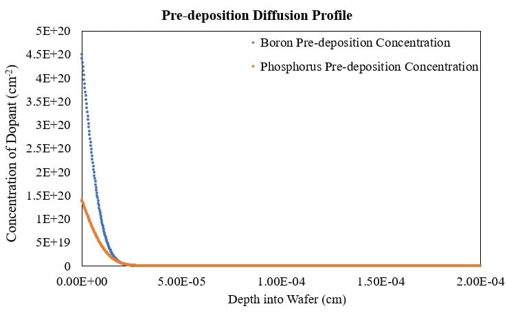
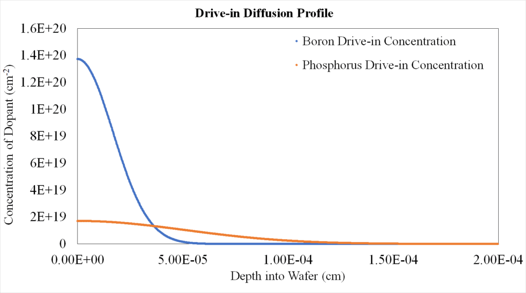
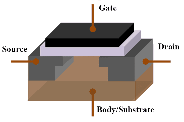
Using solutions of Fick’s second law, we can find the dopant concentration for both the pre-deposition and drive-in processes C and Cd , respectively.
Pre-deposition concentration
Drive-in concentration
Diffusivity at given temperature
![]()
where:
Cs = Surface concentration of dopant (0 – 8 × 10⁻⁴ cm-3 )
z = Distance from wafer surface (0 – 8 × 10⁻⁴ cm)
D0 = Maximum diffusion coefficient (0 – 3.9 cm2/sec)
k = Stefan-Boltzmann constant (8.6173 × 10⁻⁵ eV/K)
Ea = Activation energy of the vacancy/interstitial (Phosphorus: 3.66 eV, Boron: 3.46 eV)
t = Process duration (0.5 – 2 hrs)
T = Process temperature (900 – 1200 °C)
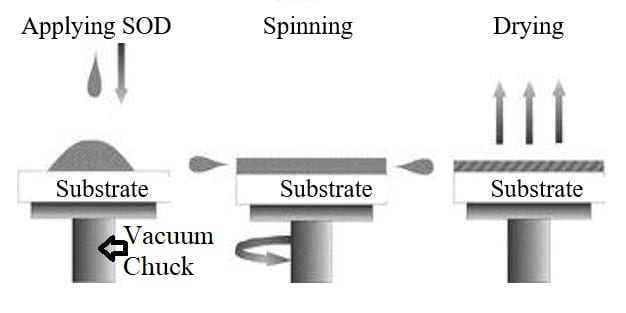
Assumptions:
○ Infinite and constant dopant concentration at the surface
○ Constant activation energy
○ No SiO2 growth during processing
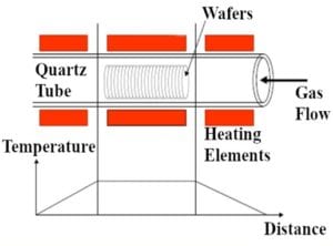
Bottom: Graph showing the relationship between the furnace temperature and distance along the furnace tube axis.5
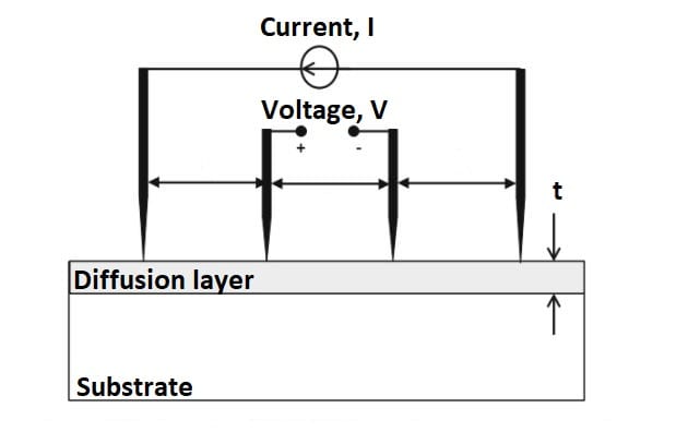
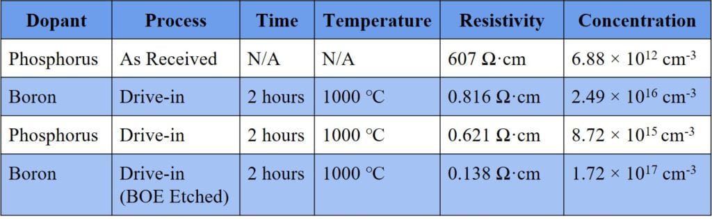
Sheet Resistance
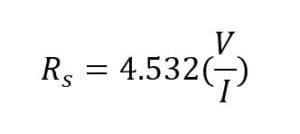
where:
Rs = Sheet Resistance
V = Voltage
I = Current