Our Team
Materials engineering students with an interest in micro electronic mechanical systems.

Daniel Gonzalez
I enjoy exploring new areas of renewable energies and research in the micro electronics industry.

Huy Le
I am interested in designing cheaper and more efficient device fabrication methods.
Acknowledgements
Thank you to our project advisor: Dr. Jean Lee.
Microfabrication Lab Directors: Dr. Hawkins, Dr. Mayer.
MATE Faculty: Eric Beaton
The MATE Department
Characterization of Thermal Diffusion Profiles of Boron and Phosphorus Dopants
in Silicon and Silicon Dioxide
Problem Statement
Ion implantation is typically used for semiconductor doping in industry, but it is expensive and unavailable at Cal Poly. At Cal Poly, doping is performed using thermal diffusion, a cheaper process, but diffusion characteristics are unique to each microfabrication laboratory and furnace. In order to better predict and understand devices fabricated in Cal Poly’s Microfabrication Lab, characterization of boron (B) and phosphorus (P) diffusion in silicon (Si) and silicon dioxide (SiO2) based on doping processes used in Cal Poly’s Microfabrication Lab is essential.
Background
Dopant Diffusion in Silicon
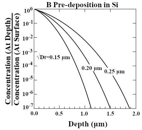
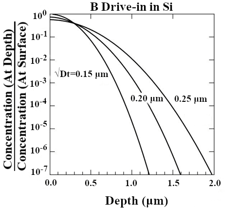
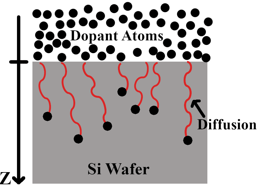
Doping silicon for device purposes without the use of an ion implanter is often achieved through two heat treatment processes. The first of these is the pre-deposition process, where the dopant is introduced onto the surface of the wafer (Figure 1). The dopant atoms usually do not travel deep into the wafer during this process. The second process is drive-in, where the dopant atoms distribute more evenly and deeper into the wafer (Figure 2). This is where the final diffusion depth of the dopant atoms will be determined. Because the drive-in process relies on the pre-deposition process, both of these processes must be characterized to garner a full dopant diffusion profile.
Dopant Diffusion in Silicon dioxide
SiO2 is a commonly used diffusion barrier in silicon microfabrication. It inhibits dopant diffusion through two primary mechanisms:
○ Formation of large immobile compounds such as borosilicate glass and phosphosilicate glass that impinge dopant atom movement.
○ Low diffusivity and high solid solubility concentration of dopants. Though noticeable in boron and phosphorus doping, it is the sole mechanism when doping with sodium, gallium, zinc, or nickel.
Simulation
Fick's Laws
A MATLAB script based on Fick’s laws of diffusion was developed to simulate the pre-deposition and drive-in processes. Fick’s laws describe diffusion of atoms through a non-porous medium. The simulation considered the ramp-up and cool-down processes, effects of oxidation, and the temperatures and durations of the pre-deposition and drive-in processes (Figure 3). The script allowed for simulation of processes with a larger range of times and temperatures than was possible in the Cal Poly microfabrication laboratory’s diffusion furnace.
Using solutions of Fick’s second law, we can find the dopant concentration for both the pre-deposition and drive-in processes C and Cd , respectively.
Pre-deposition concentration

Drive-in concentration

Diffusivity at given temperature
![]()
where:
Cs = Surface concentration of dopant (0 – 8 × 10⁻⁴ cm-3 )
z = Distance from wafer surface (0 – 8 × 10⁻⁴ cm)
D0 = Maximum diffusion coefficient (0 – 3.9 cm2/sec)
k = Stefan-Boltzmann constant (8.6173 × 10⁻⁵ eV/K)
Ea = Activation energy of the vacancy/interstitial (Phosphorus: 3.66 eV, Boron: 3.46 eV)
t = Process duration (0.5 – 2 hrs)
T = Process temperature (900 – 1200 °C)
Assumptions:
○ Infinite and constant dopant concentration at the surface
○ Constant activation energy
○ No SiO2 growth during processing
Materials
Silicon-On-Insulator (SOI) Wafers
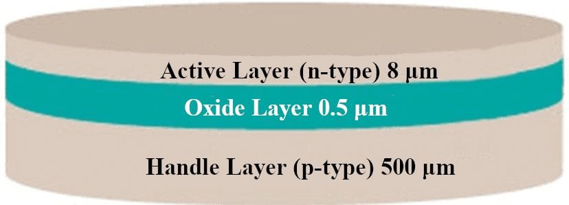
SOI wafers have an embedded SiO2 layer grown between an active Si layer and a handle (or substrate) Si layer. The embedded oxide in an SOI wafer is useful in testing the effectiveness of SiO2 as a diffusion barrier.
SOI Samples

Due to the limited number of SOI wafers available, each wafer was cleaved into 8 pieces. This generated enough samples for testing a variety of processing parameters. By changing some of the processing parameter values, we are also able to characterize the effects of the pre-deposition process on the drive-in process.
Spin-on dopant (SOD)
SODs were used as the dopant source during pre-deposition, because Cal Poly does not have the facilities to dope wafers using a gaseous source. For the boron-doped samples Filmtronics B155 SOD was used, and for the phosphorus-doped samples Filmtronics P507 SOD was used.
Methods
Experiment Variables
Doping Process:
○ Pre-deposition and drive-in
Heat Treatment Parameters:
○ Time: 0.5 – 2 hours
○ Temperature: 900 ºC – 1200 ºC
Type of Dopant:
○ Boron or phosphorus
wAfer Cleaning
All wafers and samples were cleaned before processing using the following steps:
○ Immerse in a 70 ºC piranha bath [H2SO4 : H2O2 (9:1)] for 10 minutes to remove organic impurities
○ Quench in room temperature deionized (DI) water
○ Immerse in a buffered oxide etchant (BOE) at room temperature for 30 seconds to remove surface oxides
○ Quench in room temperature DI water
○ Spin, rinse, and dry (SRD) using an SRD machine
All samples were cleaned again after each heat treatment process by immersion in BOE followed by a DI water quench.
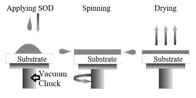
SOD Application
A spin coating process was used to quickly apply a uniform layer of SOD on top of the active layer of the SOI wafer (Figure 6).
Heat treatment
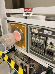
The samples were heat treated in a dopant diffusion furnace in the Cal Poly Microfabrication Lab (Figure 7). This furnace consists of a tube furnace with a quartz tube. A schematic of the diffusion furnace is shown in the top portion of Figure 8. The bottom portion of Figure 8 shows the relationship between the furnace temperature and the distance along the furnace tube axis. Placing samples near the ends of the furnace is avoided, as the temperature is not constant in these regions of the tube.
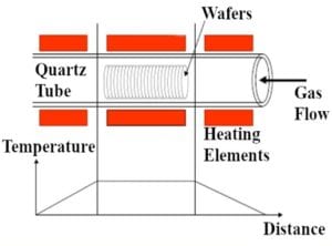
Bottom: Graph showing the relationship between the furnace temperature and distance along the furnace tube axis.5
Heat Treatment Conditions:
○ Loading temperature: 900 ºC
○ Loading and unloading speed: 30 cm/s
○ Furnace atmosphere:
• Ultra high purity (UHP) N2 gas at 6 liters per minute (LPM) during ramp-up and cool-down
• UHP O2 gas at 6 LPM during processing
Four-point probe
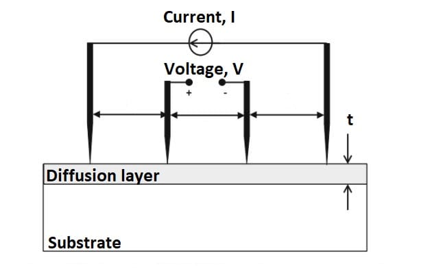
The four-point probe measures the sheet resistance of semiconductor samples by passing current through the outer two probes and measuring the voltage drop between the two inner probes (Figure 9). The sheet resistance is found by measuring the ratio of the voltage drop (mV) to the input current (mA). This ratio is multiplied by a constant that is dependent on the spacing of the probes and the thickness of the wafer; a value of 4.532 is used for this constant for the four-point probe in the Cal Poly Microfabrication Lab. The sheet resistance value can be multiplied by the thickness of the Si diffusion layer (8 µm) to find the resistivity. This resistivity value is used to calculate the dopant concentration near the surface in contact with the four-point probe.
Sheet Resistance
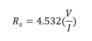
where:
Rs = Sheet Resistance
V = Voltage
I = Current
Groove and Stain
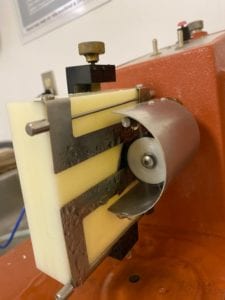
The groove and stain method is intended to reveal the junction depths of the boron and phosphorus-doped Si samples. The Signatone model S-1100 groove and stain apparatus used in the Cal Poly Microfabrication Lab is used to polish a groove into the surface of the wafer sample to expose a cross section of the sample (Figure 10).
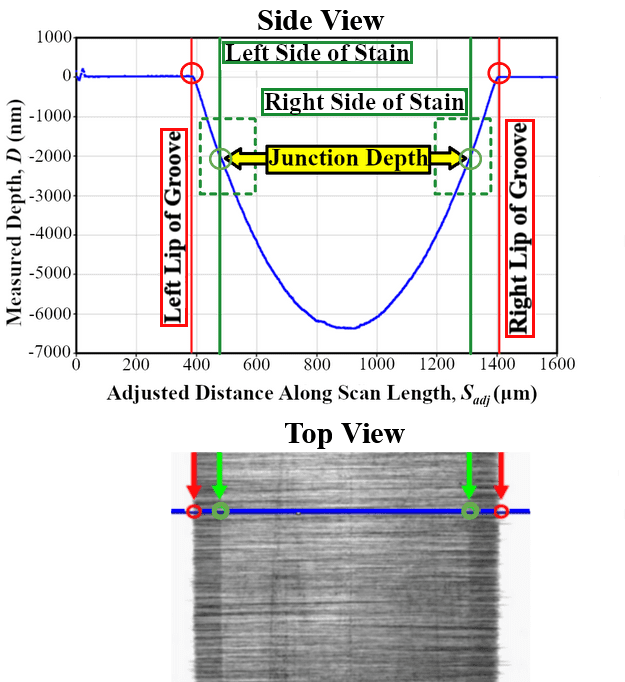
The exposed grooved surfaces of the samples were measured using a profilometer to provide the groove depth and scan length (Figure 11). Next, the samples were stained in a BOE solution for 30 min, then cleaned and rinsed. Then, microscopy images of the grooved and stained samples were taken. The junction depth is found by cross-referencing the distance between the left or right lip of the groove and the left or right side of the stain in the light microscope image with the profilometer scan.
Results and Discussion: Experiments
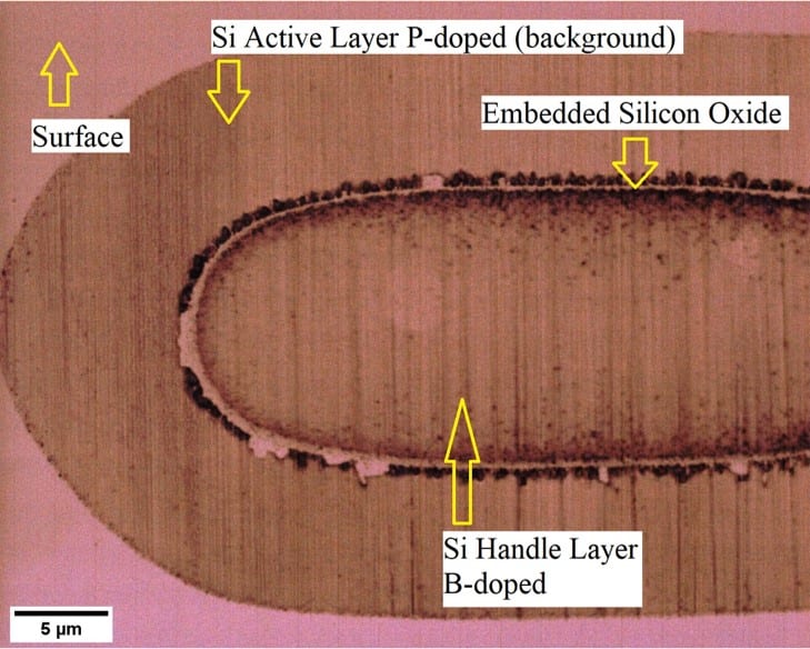
Results for junction depths of boron samples were inconclusive as it was difficult to see the junctions. This was due to poor staining of the boron-doped region, and without a distinct junction, accurate measurement could not be made (Figure 12). Additional optimization of the etching process time, temperature, lighting, and etchant concentration are needed for the staining procedure to help make the junction more easily visible. There was insufficient time to make these optimizations to the staining procedure.
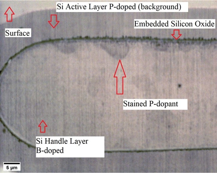
However, there is evidence to suggest that phosphorus dopants may have penetrated through the embedded SiO2 layer (Figure 13). This may be a result of the diffusion of the phosphorus dopants that are present in the background of the active layer just above the SiO2 layer. Further analysis needs to be done to justify this hypothesis.
The calculated surface resistivity and dopant concentration of the samples significantly changed compared to that of an untreated wafer (Table I). This suggests that dopant diffusion took place, but due to poor staining a distinct junction could not be measured.

Results and Discussion: Simulation
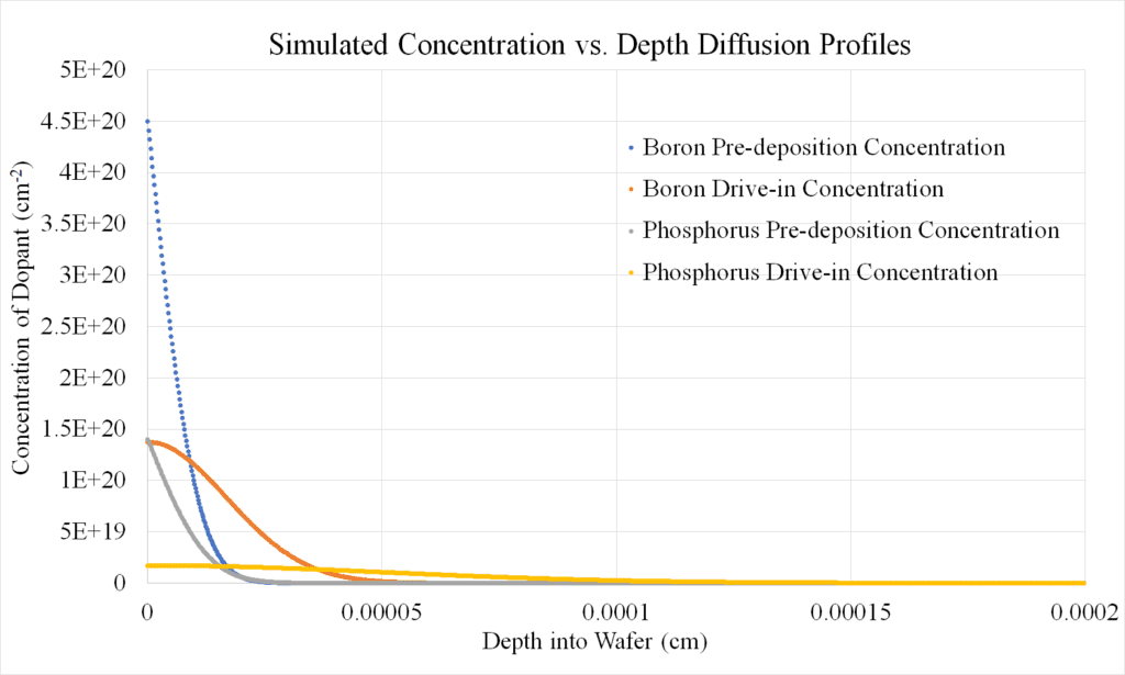
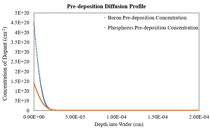
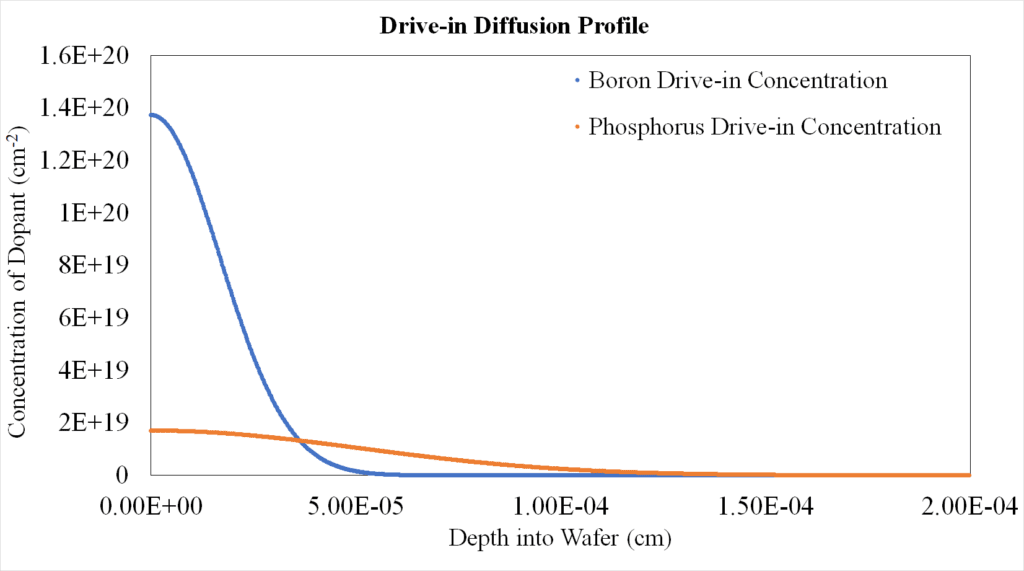
Diffusion simulation results were generated for a larger range of temperatures and durations than that of the experiments, 900 ºC to 1350 ºC and 0.5 hours to 12 hours, for both the pre-deposition and drive-in processes. As expected, the pre-deposition profile had a much higher possible maximum dopant concentration value, and the pre-deposition dopant diffusion profile was steeper than the drive-in dopant diffusion profile.
Pre-deposition Profile Results:
For a 1 hour pre-deposition process at 1000 °C, the junction depths were similar for boron and phosphorus dopants (Figure 14). This was unexpected as the diffusivity of phosphorus in silicon was much higher than boron in silicon, by up to a factor of 3. These similar junction depths were likely caused by the high solid solubility and the low diffusivity of boron in silicon in conjunction with the low maximum solid solubility and high diffusivity of phosphorus in silicon. The maximum concentration for each dopant for each of the pre-deposition and drive-in processes can be observed at the surface of the wafer (Figures 14 and 15). The boron pre-deposition concentration profiles displayed higher maximum dopant concentrations due to boron’s solid solubility in silicon being about one full order of magnitude larger than the solid solubility of phospohrus in silicon.
Drive-in Profile Results:
Comparing the drive-in processes for boron and phosphorus dopants at the higher temperature of 1100 ºC for 2.5 hours, it was observed that the junction depth from the higher temperature drive-in process was greater in the phosphorus profile than in the boron profile (Figure 15). Phosphorus was also more evenly distributed in the silicon in comparison to boron. This is likely due to the diffusivity of phosphorus being more sensitive to temperature.
Boron vs. Phosphorus:
In comparison to boron, phosphorus often produces much deeper junction depths and has higher diffusivity. This is attributed to the intrinsic diffusivity of phosphorus being much larger than that of boron. When both dopants underwent the same processing, the calculated extrinsic diffusivity of boron was two orders of magnitude larger than that of the phosphorus extrinsic diffusivity. The phosphorus intrinsic diffusivity was one order of magnitude larger than the boron extrinsic diffusivity. This contributes to the overall total diffusivity of phosphorus being consistently larger than that of boron by up to 19% at a given temperature. The increased diffusivity also allows phosphorus to generate deeper junction depths when undergoing the same processing conditions.
- Because the total diffusion coefficient of phosphorus was comprised mostly of its intrinsic diffusion coefficient, the diffusion coefficient of phosphorus in silicon was mostly unaffected by the phosphorus dopant concentration in the wafer during processing. In comparison, boron’s total diffusion coefficient in silicon was comprised largely of its extrinsic diffusion coefficient. Therefore the diffusion coefficient of boron was heavily influenced by the boron dopant concentration present in the wafer during processing.
Future Work
In the future, an improved staining procedure and further analysis of dopant diffusion from n-type active regions across SiO2 layers in SOI wafers are required to characterize dopant diffusion profiles.
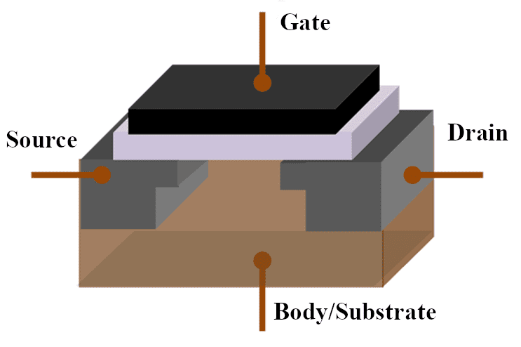
Results from this project can also be compared with dopant diffusion profile data from UC Santa Barbara’s secondary ion mass spectroscopy (SIMS) laboratory. Data generated from SIMS can be used to confirm the accuracy and precision of results generated in this project. More accurate simulations can be done using the Synopsys Sentaurus Technology Computer Aided Design (TCAD) program. Further research in the thermal diffusion doping process can improve the fabrication of more complex devices such as metal-oxide semiconductor field effect transistors (MOSFETs) or ion-sensitive field effect transistors (ISFETs) in the Cal Poly Microfabrication Lab (Figure 16).
References
- 1) Adapted from: Campbell, S. A., & Campbell, S. A. (2013). Fabrication engineering at the micro and nanoscale. New York: Oxford University Press.
- 2) Adapted from: Jones, S. W. (2008). Diffusion in Silicon. Georgetown, MA: IC Knowledge LLC.
- 3) Adapted from: S Larki, F. (March, 2018) Researchgate. Retrieved April 22, 2021 from https://www.researchgate.net/publication/323998073_THESIS.
- 4) Adapted from: Mishra, A., Bhatt, N., & Bajpai, A. K. (2019). Micro and Nano Technologies (pp. 397–424). Elsevier. Retrieved April 20, 2021 from https://doi.org/https://doi.org/10.1016/B978-0-1 2 -815884-5.00012-0. June 3, 2021.
- 5) Adapted from: Safizan (2017). Lecture notes. Retrieved April 22, 2021 from http://portal.unimap.edu.my/portal/page/portal30/
Lecture%20Notes/KEJURUTERAAN_MIKROELEKTRONIK/Semester%201%20Sidang%20Akademik%20201718/EMT%20357%20Fundamental%20of%20Microelectronic%20Fabrication/Lecture%20Notes.
- 6) Stain and Groove Diffused Dopant Depths Materials Engineering, Cal Poly State University, San Luis Obispo, CA Microfabrication Lab, Signatone Model S-1100, Standard Operating Procedure (n.d.). 2017.
- 7) Adapted from: MOSFET. (2021, April 18). Retrieved April 22, 2021 from https://en.wikipedia.org/wiki/MOSFET.
- 8) Huff M. (2020) Metrology for Microsystems Manufacturing. In: Process Variations in Microsystems Manufacturing. Microsystems and Nanosystems. Springer, Cham. https://doi.org/10.1007/978-3-40560-1_5.

